Chemical etching vs laser cutting, which one works best?
This is a question we’re often asked as both methods offer cost-effective, precision cutting and engraving of sheet metal, so which one would work best for you?
The key difference is material thickness, anything less than 1.5mm and chemical etching generally wins the day, with new advancements in digital tooling, etching is far more flexible in terms of turnaround, cost, and volume with a consistent accuracy down to 25 microns.
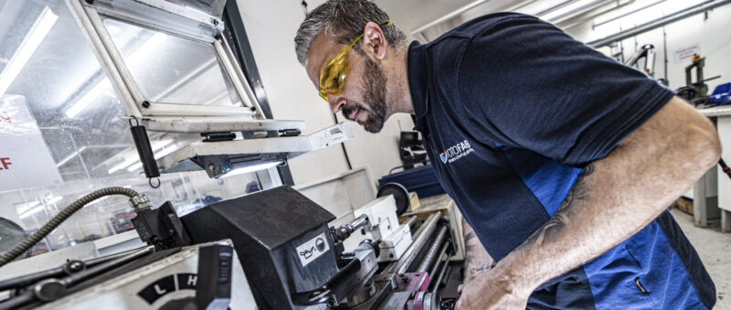
Photofab have been experts in chemical etching for over 50 years offering a broad range of capabilities to ensure the customer gets exactly what they need and when they need it. Working alongside our strategic partners, we can also provide an extremely competitive laser cutting service for those thicker materials. Take a look at both services in more detail and decide for yourself.
In the red corner: chemical etching
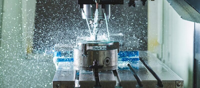
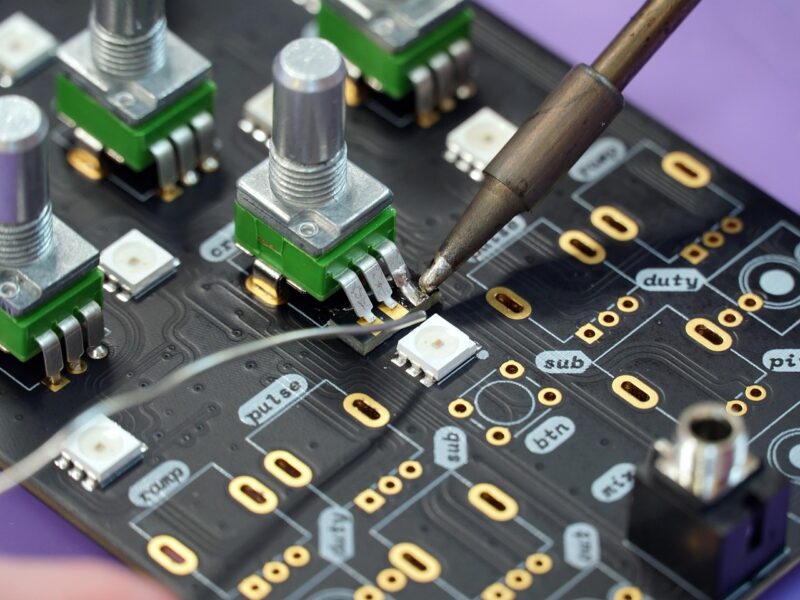
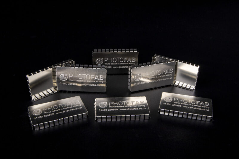
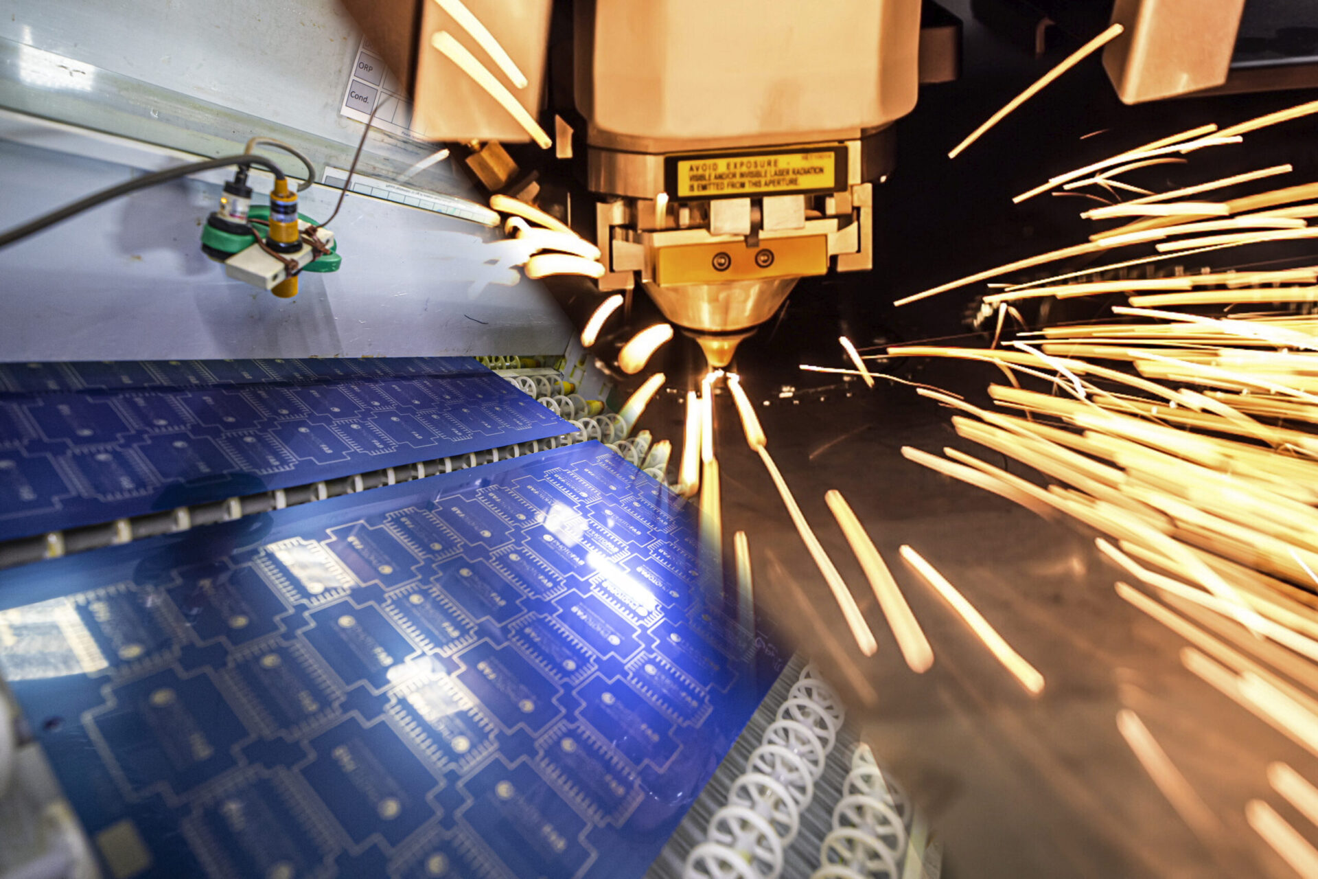
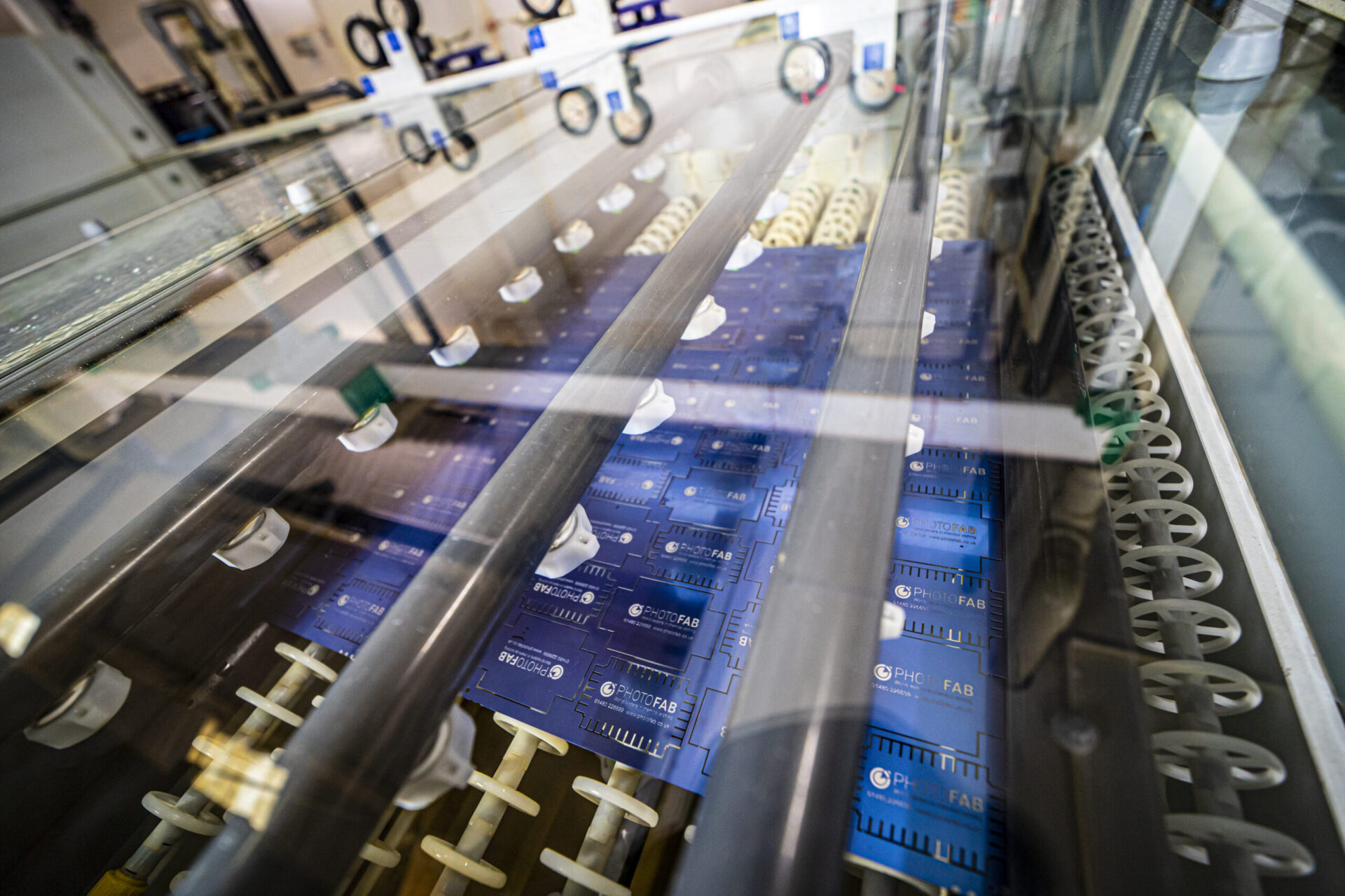
Chemical etching is a machining process for producing precision components which uses acids and other chemicals to erode unwanted metal. From our headquarters, Photofab can work with a wide range of metals, such as brass, copper, beryllium copper, stainless steel, carbon steel and mild steel up to a thickness of 1.5mm.
All in the detail
For quality and precision, chemical etching is still one of the industry favourites, etching maintains incredible tolerances and accuracy, with detail and intricacy that still amazes us.
High volume production
For fast turn-around and mass-production, chemical etching is the perfect choice as many parts can be etched simultaneously, saving valuable time and money. Thanks to our refined chemical etching process, the final pieces are burr-free and leave the material structure completely unaltered, ideal for electrical and electronic applications.
Low volume and prototyping
For prototyping, a combination of digital tooling, automated etching and finishing processes allow for quick and easy design changes to be made, making chemical etching the favoured choice for flexibility and lead-times.
Shaping up nicely
As part of our full-service offering, we also have a dedicated engineering division for forming and finishing with a stock of 1000’s of hard tooling to cover a multitude of shaping requirements. If there are bespoke forming requirements, we can also manufacture specific tools in-house to drive down costs and speed of turnaround.
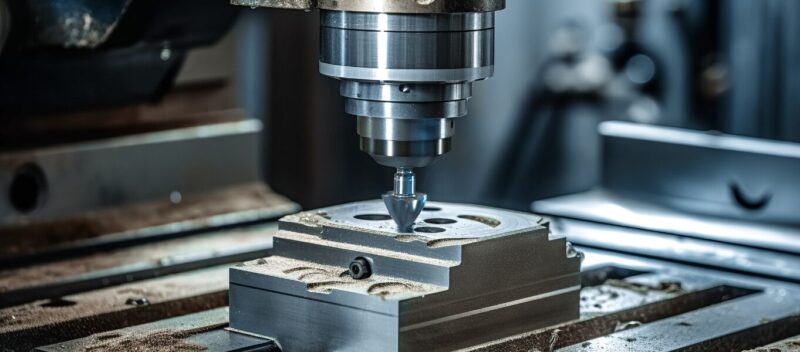
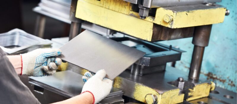
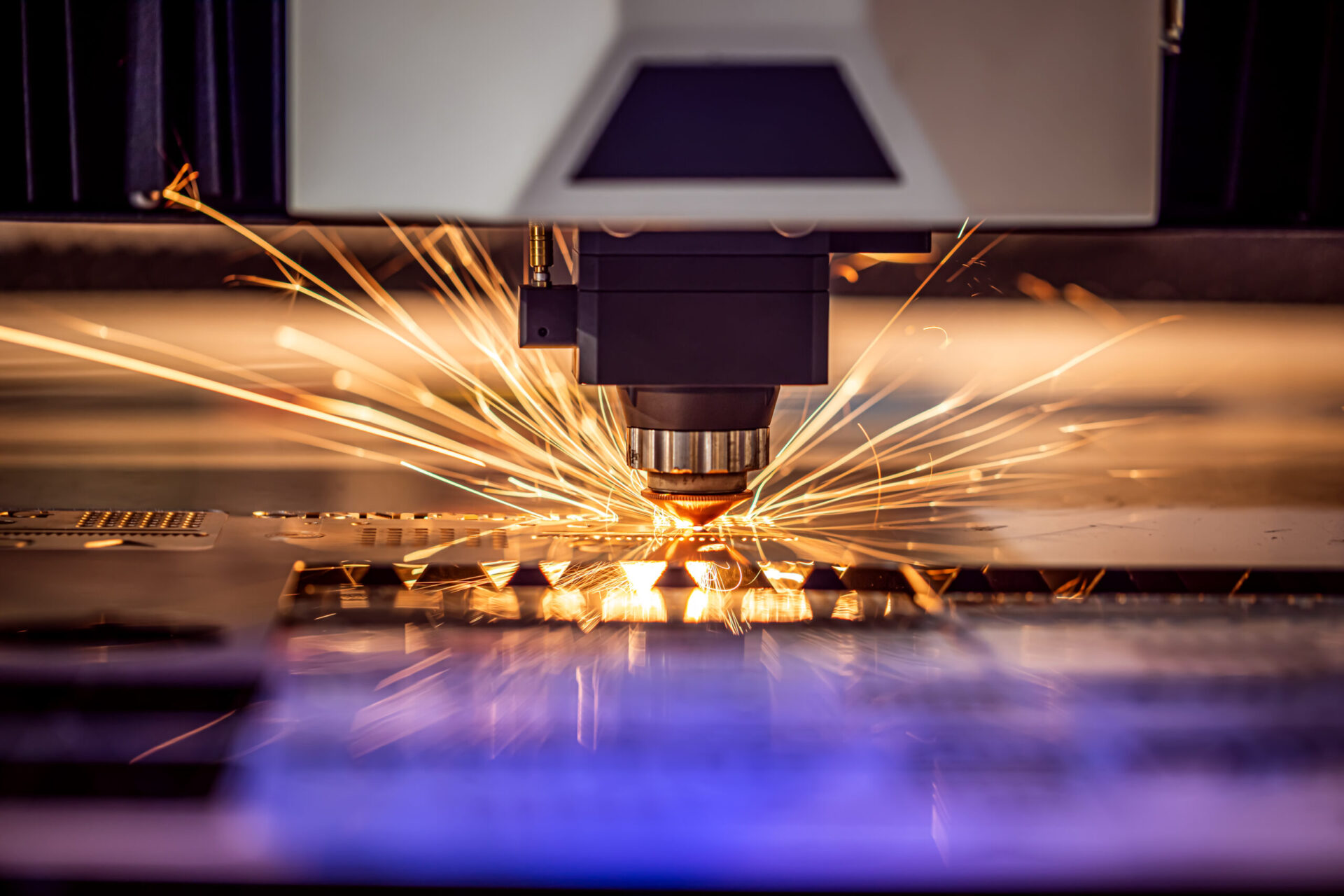
In the blue corner: laser cutting
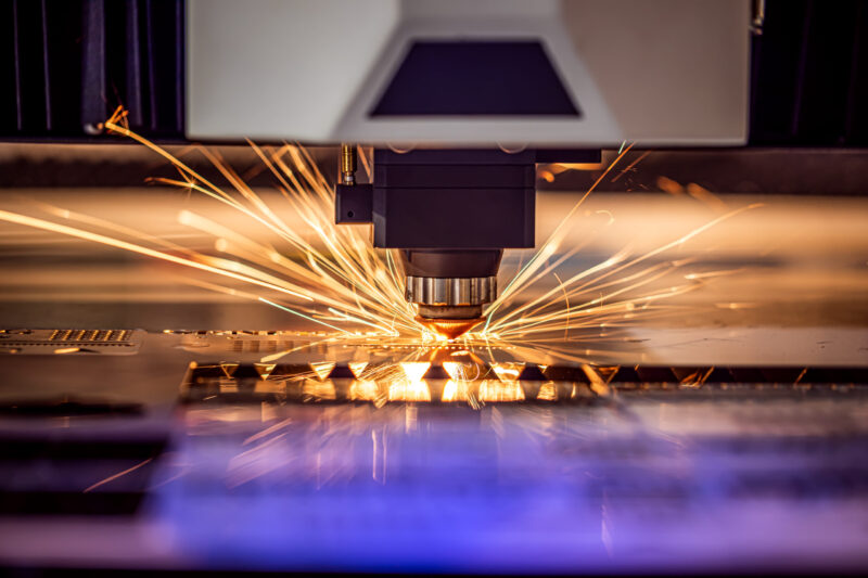
Laser cutting does exactly what it says on the tin: uses a laser to cut through metal. The process works by directing the output of a high-power laser through the metal, which will either burn, melt or be blown away by a jet of gas, leaving the edge with a high-quality surface finish.
Pin-point accuracy
The precision of laser cutting is a key factor, as the laser beam does not wear away during the process. This results in laser cutting providing highly complex designs that are ideal for short run jobs, rather than high volume mass production. Simply put, if you are seeking a solution for small volume work over 1.5mm, laser cutting is the perfect technique.
Thick as you like
Well, up to 22mm anyway, laser cutting is by far the favoured method for thicker metals and provides great accuracy on a large range of metals, which can be highly cost effective and offers short lead-times. Perfect for lower volume production over 1.5mm thick.
Red or blue Photofab is always the best choice
Thanks to Photofab’s capabilities and supply chain management, whichever route you choose, you are guaranteed a great service. From prototyping to mass production, using Photofab’s in-house chemical etching service provides the perfect choice for precision and short lead-times for sheet metals under 1.5mm thick. For precision and low volumes over 1.5mm, laser cutting is the better option, reassuringly managed and quality controlled by Photofab to the exact same high standards.
No matter what you choose, all of our processes follow SC21, ISO9001, 14001 and 45001 with full traceability along the way. Our experience, coupled with our vast range of industry leading equipment and trusted network of partners makes Photofab the perfect choice for precision manufacturing, whatever your requirements.
Positives of Chemical Etching
When it comes to manufacturing intricate, high-quality metal parts, chemical etching is a standout solution. This advanced, non-invasive technique offers unique benefits that make it the method of choice for industries as varied as aerospace, electronics, medical devices and beyond. But what exactly sets chemical etching apart?
Protecting Material Integrity
One of the standout benefits of chemical etching is its non-contact nature. Unlike mechanical methods such as stamping or laser cutting, chemical etching relies on a controlled chemical process to dissolve unwanted parts of the material. This means there’s no risk of tool contact, which could otherwise cause stress or deformation to the workpiece.
For industries requiring exacting standards, such as aviation or healthcare, avoiding mechanical stress is paramount. Components maintain their original material properties, ensuring better durability and reliability in their applications. This is especially beneficial for metals like stainless steel, where preserving material integrity is essential.
Precise at Thin Tolerances
When working with thin metals under 1.5mm thick, precision is key and this is where chemical etching really shines. The process delivers unmatched fidelity for intricate and miniature designs. Whether it’s tiny micro-holes in electronic components or fine pieces of a mobile phone camera, chemical etching enables manufacturers to bring complex ideas to life.
This level of precision is particularly valuable in electronics and medical device industries, where components often feature delicate, intricate details. Customers in these sectors can count on chemical etching to meet rigorous specifications without compromise.
Burr-Free and Smooth Edges
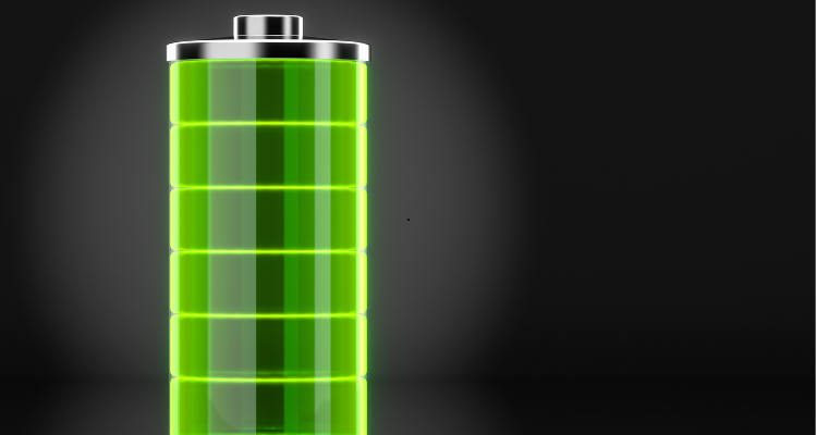
Nothing derails the production process like the need for additional finishing. Thankfully, chemical etching eliminates this concern by producing parts with burr-free, smooth edges. The absence of sharp edges or residual burrs makes it perfect for components that require high aesthetic or functional precision, such as battery parts or sensitive medical devices.
For industries where cleanliness and safety are paramount, burr-free edges provide a clear advantage. Not only does this save time, but it also ensures the final product meets the highest standards.
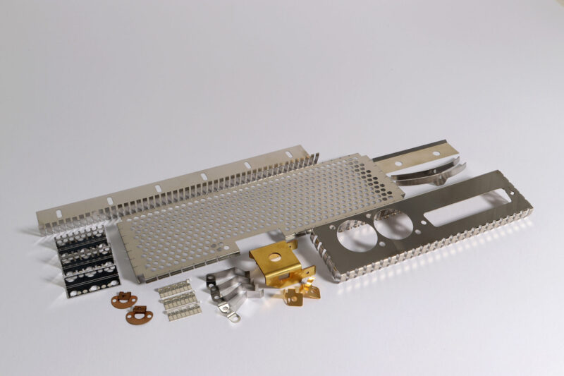
Ideal for Complex Geometry Demands
When it comes to intricate designs or multiple fine cut-outs, chemical etching outperforms other methods. The beauty of this process lies in its simplicity for complex geometries. Unlike machining or stamping, where increased complexity often means higher costs and production times, chemical etching handles intricate features with ease and without any added expense.
For designers and engineers, this opens up endless possibilities for innovation. Whether it’s a perforated metal component for filtration systems or a delicate electronic shield, chemical etching makes even the most ambitious designs a reality.
This efficient, cost-effective way of producing fine metal components helps to keep costs low when producing large quantities of small-scale parts. Whether you’re producing a batch of 50 or 50,000 components, chemical etching keeps both production time and costs in check.
Use Cases of Chemical Etching and Laser Cutting
When it comes to precision manufacturing, both chemical etching and laser cutting offer unique advantages tailored to different needs. Understanding their specific use cases can help businesses make informed decisions for their projects. Below, we break down the strengths of each method to guide your choice.
Chemical etching excels in producing high-precision components with intricate details. Its ability to create parts for EMI/RFI shielding is vital in industries like electronics, where interference needs to be minimised. Similarly, it’s commonly used for fine mesh filters or screens that require precise apertures for optimal functionality.
This method also leads in producing parts from hard-to-machine metals such as stainless steel or nickel alloys. Where tight tolerances are critical, chemical etching delivers perfect results without any material distortion or stress. Examples include microfluidic plates, heat exchanger foils and other high-performance components.
Laser cutting is distinguished by its ability to handle thicker materials with ease. It’s highly effective for cutting metal sheets between 2mm and 25mm, making it a key choice for heavy-duty applications. Automotive parts like chassis components, brackets, and structural supports often benefit from the precision and speed of this method.
Its quick setup and lack of tooling make laser cutting the go-to solution for rapid prototyping or small production runs. This is particularly useful for jobs requiring quick turnarounds, such as decorative panels, signage, and custom enclosures. This method balances efficiency with exceptional accuracy, especially in small-scale projects or one-off designs.
Determining the better method ultimately depends on your project’s requirements. Chemical etching is ideal for applications involving thin metals, intricate details, or challenging materials. It’s the preferred choice for industries needing high-precision, burr-free parts, especially at higher volumes.
Laser cutting, on the other hand, excels when working with thicker materials, offering speed and adaptability. For industries like automotive, construction, or design, where robustness and quick turnarounds matter, laser cutting provides unmatched capabilities.
Reach out to our experts to discuss your options or read our guide on chemical etching versus water jetting.
FAQs: Chemical Etching vs Laser Cutting
1. What is the best method for cutting thin stainless steel?
For cutting thin stainless steel (especially below 1.5mm), chemical etching is often the preferred method. It delivers high precision, burr-free edges and maintains material integrity, ideal for industries like electronics, aerospace and medical manufacturing in the UK.
2. Is laser cutting suitable for low-volume metal part production?
Yes. Laser cutting is highly suitable for low-volume or prototype production thanks to its fast setup, digital design flexibility, and minimal tooling costs. It’s a go-to choice for bespoke or rapid-turnaround metal parts.
3. Which process is more cost-effective for high-volume precision parts?
Chemical etching tends to be more cost-effective for producing large quantities of high-precision metal parts, especially where intricate details or burr-free finishes are required.
4. Can chemical etching be used for aerospace components?
Absolutely. Aerospace manufacturers use chemical etching for lightweight, high-precision parts with complex geometries—ideal for EMI shielding, micro-perforated parts and weight-sensitive applications.
5. What are the environmental advantages of chemical etching in manufacturing?
Modern chemical etching processes in the UK are increasingly eco-friendly with recyclable etchants and waste treatments. Additionally, the process reduces mechanical waste and energy usage compared to laser or CNC machining.
Production is only a quick call away
Call one of our dedicated team of account manager’s today or contact us now to see how Photofab’s chemical etching and laser cutting services can give you the results you are looking for. You can also keep up to date by following us on LinkedIn and Twitter.
Or carry on learning and read about the different between chemical etching and water jetting.