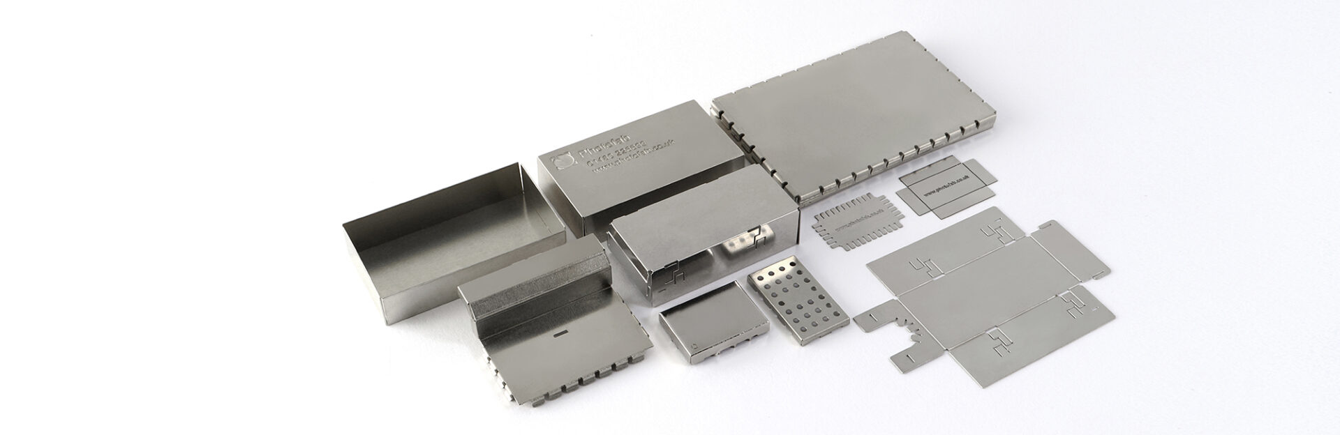
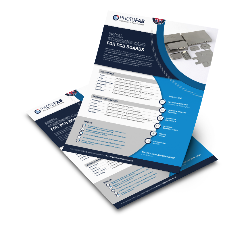
EMI / RFI SHIELDING PRODUCTS
Photofab can supply EMI / RFI shielding cans and solutions using various intelligent design techniques for use in critical infrastructure like circuit board shielding.
With over 50 years of experience, Photofab have worked closely with leading electrical and electronic manufacturers to adapt and perfect our processes, ensuring the highest standards in quality, precision, and consistency for the manufacture of EMI/RFI Shielding products.
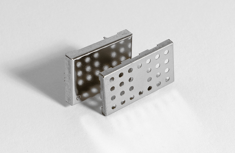
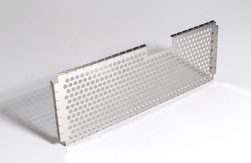
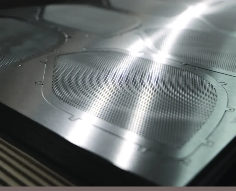
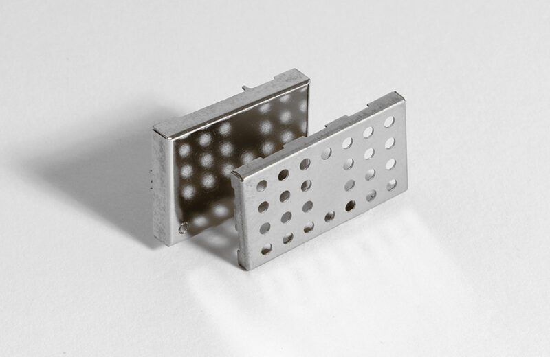
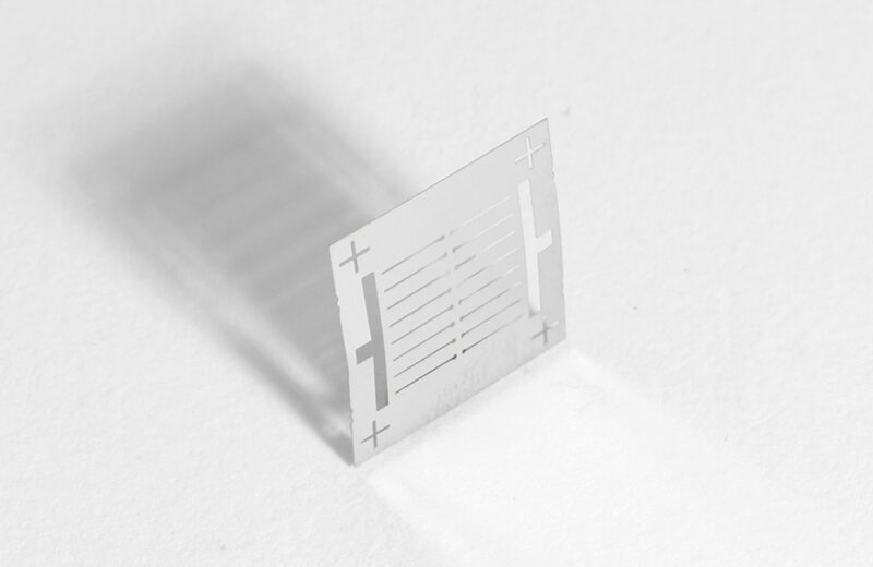
Shielding is a smart, simple technique for controlling Electro-Magnetic or Radio Frequency interference. Shielding cans are metal boxes that are applied to the board with clips or solder. Photofab has experience in producing these shields. These shields are most commonly applied to parts of a circuit that have high EMI emissions or are sensitive to inference.
Shielding or screening cans are commonly manufactured in Nickel Silver, as it maintains solderability with no post coating required, or traditionally in either brass or mild steel plated with either tin or nickel, depending on what suits your application best. The full process is available, including forming, plating, soldering and / or spot welding.
For more information on how we can reduce your costs & improve lead time contact our dedicated account managers on 01480 226699 or email enquiries@photofab.co.uk.

EMI and RFI PRODUCT FEATURES with Chemical Etching
Solder Joints
Butt jointed corners with tin plate finish, allows corners to be soldered for increased screening, where frequency dictates.
Spot Welding
Overlapping joint corners with tin plate finish are spot welded for increased screening, where frequency requirements dictate.
Locking Tabs / Locating Holes
an alternative to soldering, allowing greater rigidity depending on the needs of the application.
Dividers
provide discreet screening within the frame.
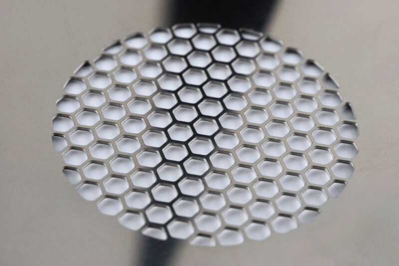
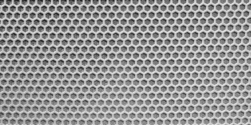
Holes / Cut Outs
can be incorporated as requested,
Anti-Solder Migration Barrier
prevents solder creepage up the sides of its PCB mounting screening enclosures during automated and reflow soldering processes.
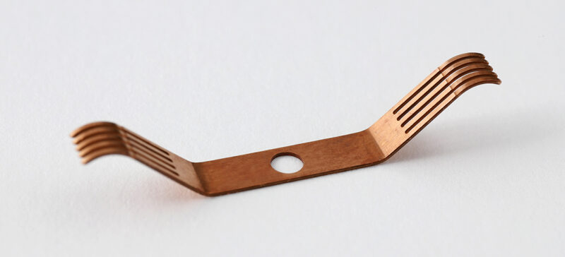
Spring Fingered Lids
easy access and excellent attenuation – our in-house designed spring fingered lids come from standard tooling and provide easy access and excellent attenuation.
Push Fit Lids
easy access and good attenuation.
PCB Locations
lancings or brackets can be specified to act as guides or supports.
Locking Pins
for exact positioning and retention, deal for reflow soldering applications.
Half Etch Pins
pins that are easily bent, to lock the shielding can into place.
Common Metal Types
Copper, Brass, Mild Steel, Stainless Steel, Nickel Silver and Mu Metal.
Common Plating Types
Tin plate (Bright and Electrolytic) and Nickel plate.
RoHs Compliance
All standard metal used for shielding cans are RoHS compliant. The types of plating we offer will always be RoHS compliant, unless you state otherwise. Please note that Hot Tin Dip is not RoHS compliant.
Benefits of CHEMICALLY ETCHED EMI / RFI Shielding
EMI / RFI shielding at PCB board level is a deceptively simple technique for controlling EMI (Electro-Magnetic Interference). It is perhaps the most common technique to keep harmful interference out and also unwanted emission in. EMI shielding at PCB level is simple to engineer with low cost. Board level shielding solutions can be used to achieve an EMI performance that would be far more difficult and costly at product enclosure level.
At board level, shielding cans can be used selectively on problem areas of a circuit, directly tackling components with emissions that are too high or are too sensitive.
In brief, PCB shielding cans are simple metal boxes that are easily soldered in place. Dealing with EMC problems at this level, ensures component and assembly costs are low and the appearance and ease of maintenance of the product are not compromised.
Why is Enclosure level at product level inferior in EMI sheilding?
Practical EMI shielding requires considerable engineering skill to give good results. However, at product enclosure level, it can be complex and expensive when considering both additional material and assembly costs. Also, effective enclosure shielding usually requires substantial filtering of all cables, which pass out of the product right at the point where they penetrate the enclosure shield.
Shielding at PCB Level
Simple to engineer
Low-cost
High EMI performance achievable
Tackle problematic components directly
Shielding a Product Enclosure Level
Considerable engineering required
High Cost due to complexity
Additional materials required
Filtering for cables required
Effect on emissions
With the PCB shielding method of execution, the circuit board tracking and wiring is shielded inside the can solution. Due to space, contained tracks and wires are consequently very short and not very efficient as aerial radiating RFI or EMI. Furthermore, filtering to reduce overall emissions to an acceptable level, may be minimal if required at all.
The benefits of
working with us
We are world leaders in the development of photochemical technology to produce intricately shaped components. We have produced over 80,000 different components over the years and are highly regarded for our chemical etching process. Our engineers offer many services, and will offer advice to improve the product and reduce the costs.
24-hour quotation service
Dedicated account managers
Rapid manufacturing service
Cost saving stock of uni-tooling
Etched fold lines for tool-free forming
Full manufacturing service and supply chain management
Access to manufacturing and technical advice and expertise
Quality accredited to ISO 9001, ISO 14001, ISO 45001 and SC21 Bronze
TAKE A LOOK AT OTHER
PRODUCTS FROM PHOTOFAB
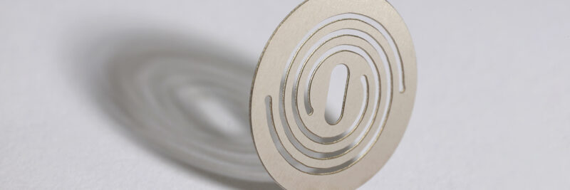
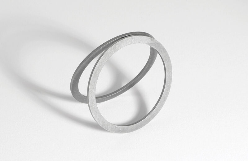
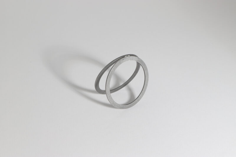
Formed Components
We can be your all-in-one supplier of metal parts. In addition to manufacturing your parts we are able to offer a variety of forming solutions to suit your individual needs.
Metal Laminations
Photofab use their industry-leading chemical etching along with a range of post processes to supply metal laminations of the highest quality.
Speaker Grilles
At our state-of-the-art facility, we employ cutting-edge chemical etching techniques to create custom speaker grilles for many different industries and applications, including automotive, stereos and other sound devices.
EMI / RFI Shielding Products
We can supply EMI / RFI Shielding cans and solutions using various intelligent design techniques.
Filters, Meshes, Screens & Grids
We have a wide experience in the manufacture of metal meshes, filters, screens and grids.
Metal Fuel Cell Plates
Our automotive unit work with many leading car manufacturers in the quest for zero emissions through fuel cell plate technology, helping to support innovations in PEM hydrogen fuel cells.
Electrical Contacts & Connectors
Chemical Metal Etching is an ideal manufacturing process for electrical and electronic components requiring incredibly tight tolerances.
Encoder Discs and Actuators
We understand the need for high accuracy, fine apertures, no burrs and additional coatings.
Burr-free Precision Components
Chemical Metal Etching is an ideal manufacturing process for electrical and electronic components requiring incredibly tight tolerances.
Metal Shims and Spacers
Our shims are often used to absorb tolerances between two components, reducing incompatibilities. The whole manufacturing process is managed in-house by one of our experienced and technically trained account managers.
Gaskets & Seals
We can produce metal gaskets and seals, and regularly supply high precision custom gaskets and seals for use in multiple industries.
Masks and Stencils
We have been producing masks and stencils for industrial use for many years, backed by over 55 years of metalworking experience.
To find out how we can help you
Get in touch today